When Henry Ford reimagined the manufacturing process with interchangeable parts and a ‘continuous flow’ through specialist operators, he cut motor car production from 12 hours to 93 minutes. Replicated by manufacturers globally, this new production paradigm not only made cars affordable for the masses but drove huge social and industrial change.
A century on, by channelling Ford’s pioneering approach to processes as well as products, engineers are continuing to find solutions for today’s pressing challenges.
One of these is ‘CAD-to-FAB’ - CAD stands for ‘computer-aided design’ and FAB for ‘digitised fabrication.’ Combined, this process can streamline and clean up the entire production line, from concept to customer-ready unit.
Old ways
The production of satellite communications components provides a useful modern illustration of the step-change CAD-to-FAB represents. Like the motor car, these items were until recently, highly customised and used sparingly for only the largest and most expensive of projects. However, with the growth of low orbit satellites and other infrastructure to deliver ‘anywhere/anytime’ communications, they’ve gained a ‘mass production’ imperative – in terms of volume, cost and pace of delivery.
Not only is this impossible to achieve with traditional component development processes, but unjustifiable given their associated environmental impact.
Take Smiths Interconnect’s original route for prototyping one such component: an isolator, which is used in satellite and radar systems to ‘quarantine’ signals from electrical and environmental interference.
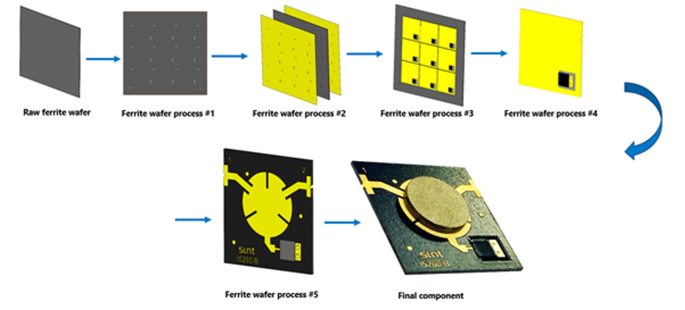
Post-design production began with 2x2-inch, unmarked ceramic, wafer-thin bases – known as wafers - similar to what’s used in your phone chip. After a quality check in Dundee, Scotland they shipped to Dallas, Texas for perforation with the tiny holes that will later ‘ground’ the electrical signals moving through them – something that’s essential for the isolator to do its job, but a time-consuming, manual task.
Next, the wafers were shipped to our site in San Jose in Costa Rica where we applied the conductive ‘thread’ through which the signals flow (typically gold or silver for their superior conductive quality).
But, because we, like all other manufacturers, lacked technology precise enough to ‘draw’ the required pattern onto the wafer, we coated all of it - using the slow, wasteful process of blasting a gold or silver ingot with a high-voltage charge until it shed sufficient tiny particles to cover both sides – before the excess material was finally etched off with acid.
Between coating and etching, the wafers were diced into individual 13x13mm isolators, ready for final assembly in Dundee. This involved the fiddly process of manually adding a magnetic circuit to each isolator. Because any imprecision undermines performance, each item had to undergo an additional manual inspection before being performance-tested in our Space Test Lab.
With new products requiring an average of 2.1 design iterations before finalisation, in total this process could see them travel some 36,000 air miles over a lengthy 26 weeks - not something we could or wanted to scale up.
“FAB” idea
Instead, we’ve developed a revolutionary ‘CAD-to-FAB’ process which has been successfully trialled on a customer order for isolators for a radar system.
It began in much the same way with Dundee and Dallas doing what they had always done; but then the Costa Rica team devised a new, speedier and cleaner way to apply the conductive material: using a high-end screen stencil to uniformly coat it. Although it still coats the whole surface, it takes just one hour per round instead of several days and wastes far less material.
The Dundee team then used patent-pending digital patterning to remove excess material – a far faster and cleaner technique than acid-etching. And final assembly is performed by COBOTs (collaborative robots) – which are far quicker and more precise than humans. Due to the tight controls embedded throughout this digitised process, the customer only required final testing of 0.1% of samples, saving further time.
The impressive outcome of the trial not only attracted a major new contract, but also match-funding from the UK Space Agency that’s now enabling the establishment of a £3.8m single-site CAD-to-FAB facility in Dundee. This final improvement means that all steps in the new process will now be performed in Scotland – removing the need to send to other international locations and saving some 25,000 air miles, 8 months and 46% of the cost of the average new product development cycle.
Grant Robertson, an engineer at Smiths Interconnect, explains: ‘This ground-breaking facility allows us to eliminate all mid-production shipping, waste and the use of acid. ‘Plus, by making design and production cheaper and more repeatable, it enables us to handle more - and larger orders with the same resource, and target higher risk/reward opportunities.’
With a patent pending for the proven CAD-to-FAB process, the team is already working to fully automate other stages of assembly and inspection. It’s this kind of drive that will help reduce our industry’s impact on the planet while scaling up innovation that improves lives. We’re pretty sure Henry Ford would approve.
How the CAD 2 FAB process works.