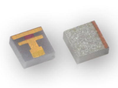
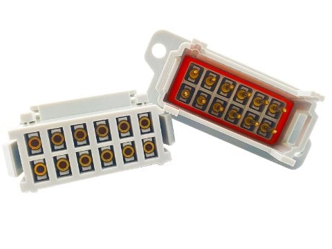
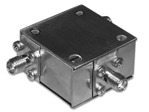
Smiths Interconnect interposers can be soldered or compression mounted enabling a reduction in manufacturing costs and providing space savings in a confined area. Interposers can be designed to handle substantial amounts of power safely with some individual contacts capable of withstanding as much as 30 Amps in free air. Spring probe technology in custom connectors allows for the integration of mixed signals and functions within a single connector design. This innovative approach enables greater versatility by combining multiple functionalities, such as power, signal, and data transmission, into one compact and efficient solution.


