Skip to content

K Series H-Pin® Socket

The K-Series socket is designed to apply flat even pressure on the DUT with a secondary lever once the lid has been closed. This is to ensure that the platen does not skid across the top of the device when closing the lid potentially marking the device. This is especially important for exposed die products, or automotive applications where appearance is part of the pass/fail acceptance criteria post test. The vertical lever actuation does not increase the overall socket footprint, allowing for the highest density of populated sites on the burn-in board and in some cases reduces the overall footprint compared to other clamshell lid sockets. Another added benefit of the K-Series lid is airflow through the socket due to the taller profile, allowing for larger air channels to help maintain accurate temperatures.

Download Brochure

Features & Benefits

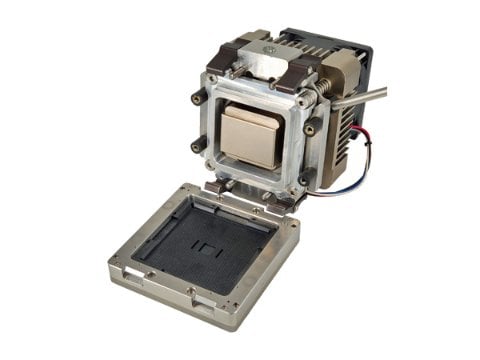
  • Industry-proven design, in-house tooling, molding, and machining, with 100% automated assembly.
  • Extensive catalog of components, configurable options
  • Zero-marking lid actuation contributes to higher yields.
  • Market-leading electrical performance

Feature options

  • Vertical pressure platen
  • Heat sink
  • HAST venting features
  • Integrated thermal control with heater and sensor
  • Reverse seating plane
  • Max component clearance under the DUT
  • 2 or 3 plate systems
  • High temperature materials for above 200°C applications

H-Pin Technology

This socket also uses the H-Pin contact technology providing wide RF performance capabilities and exceptional DC characteristics. The K-Series socket checks all the boxes: high frequency, high current, high temperature, low inductance, and Low loss. These features contribute to lower the cost of tests.

Related News

  • Widget Image ALT

    Advanced Thermal Management IC Test Solutions

    Utilizing state-of-the-art system simulation models allows Smiths Interconnect to optimize each lid’s design for efficient heat dissipation through a variety of cooling mechanisms.

  • Image of Challenges Semiconductor Package Size and Pitch Face in Shrinking Consumer Electronics

    Challenges Semiconductor Package Size and Pitch Face in Shrinking Consumer Electronics

    Tiny computers, smartphones, and small electronic devices that industry leaders and other companies have popularized are forcing the hand of semiconductor package designers to shrink the package to fit within these little hand-held gadgets. The demand for technology applications, such as smart homes, smart manufacturing, smart medical care, and automotive electronics, continues to increase. At the same time, the requirements of continuous miniaturization and functional diversification of electronic product demands also increase.

  • Image of Burn in test products

    What is thermal simulation and why is it important to reliability burn-in testing?

    Not every semiconductor manufacturer utilizes thermal simulation in their reliability testing setup. Lower power burn-in allows for an acceptable temperature rise within the package/die in a traditional burn-in chamber running at 125°C. As packages in burn-in are moving to higher power output, socket and burn-in systems may need to have enhanced features to manage the desired target die temps.