Skip to content

ES Micro Series H-Pin® Socket

ES Micro Series Socket is a technological advancement in the burn-in socket segment, with a dual latch clamshell lid to provide co-planar pressure on the DUT when the lid is actuated. The inclusion of the patented H-Pin contact technology in the ES Micro-Series socket provides market-leading electrical performance in the smallest footprint for the highest possible parallelism on a burn-in board. This series is compatible with standard heaters and temperature sensors.

Download Brochure

Features & Benefits

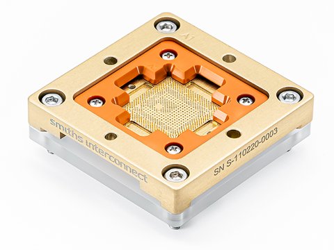
  • Configurable design, In-house tooling and molds allow for the lowest cost of test.
  • An extensive catalog of standard parts reduces cost and lead time.
  • Double-latching clamshell provides ease of use during operation and clearance for lid operation.
  • Exceptional electrical performance provides wide RF bandwidth.

Feature Options

  • LGA, BGA, and package on package
  • Spring loaded plunger
  • Heat sink
  • HAST venting features
  • Integrated thermal control with heater and sensor
  • Reverse seating plane
  • Max component clearance under the DUT
  • High temperature materials for above 200 °C applications

Related News

  • Image of  DaVinci test socket offering

    Smiths Interconnect expands DaVinci test socket offering

    The request for increased functionality in the smallest possible footprint has led to a reduction of the pitch of integrated circuits below 500 μm. At the same time, increased performances in SoCs affect pin-to-pin noise or what is commonly called crosstalk during testing.

  • Image of Challenges Semiconductor Package Size and Pitch Face in Shrinking Consumer Electronics

    BGA Sockets To Solve All Your Electronics Testing Needs

    Plastronics, a Smiths Interconnect technology brand, is a global provider of innovation for semiconductor reliability testing, meeting the industry’s burn-in socket needs for more than 40 years. It all started when our company invented the first open-top, application-specific socket for production burn-in of LCC packages. This innovation helped semiconductor manufacturers significantly increase their throughput and decrease costs.